
VRC2 pinout
Konami VRC2 and VRC4: 0.6" 40-pin PDIP (iNES Mappers 21, 22, 23, and 25)
f: connects to Famicom
r: connects to ROM
w: connects to WRAM

                      .--\/--.
       (f) CPU A13 -> |01  40| -- +5V
       (f) CPU A14 -> |02  39| -> PRG A17 (r)
       (fr) CPU Ax -> |03  38| -> PRG A15 (r)
       (fr) CPU Ay -> |04  37| <- CPU A12 (f)
       (f) PPU A12 -> |05  36| -> PRG A14 (r)
       (f) PPU A11 -> |06  35| -> PRG A13 (r)
       (f) PPU A10 -> |07  34| -> PRG A16 (r)
       (r) PRG /CE <- |08  33| <- CPU D0 (fr)
       (f) CPU R/W -> |09  32| <- CPU D1 (fr)
(CHR /CE) (r) OR Y <- |10  31| <- CPU D2 (fr)
(PPU A13) (f) OR B -> |11  30| <- CPU D4 (fr)
(PPU /RD) (f) OR A -> |12  29| <- CPU D3 (fr)
     (f) CIRAM A10 <- |13  28| -> CHR A17 (r)
       (f) /ROMSEL -> |14  27| -> CHR A15 (r)
            (f) M2 -> |15  26| -> CHR A12 (r)
  VRC4 (r) CHR A18 <- |16  25| -> CHR A14 (r)
     VRC4 (f) /IRQ <- |17  24| -> CHR A13 (r)
      VRC4 /WR9003 <- |18  23| -> CHR A11 (r)
 VRC4 (w) WRAM /CE <- |19  22| -> CHR A16 (r)
               GND -- |20  21| -> CHR A10 (r)
                      `------'

pin 3, 4: see below
pin 18: (VRC4): writing to $9003 pulls this pin low
pin 16-19: in VRC2, these pins seem to have been intended for a never-seen-used EEPROM
Konami was greatly fond of making minor variations from one game to the next, presumably to make life harder on pirates. Note that no commercial games used VRC4f configuration.
   (fr) CPU A2 -> |03  38| -> PRG A15 (r)
   (fr) CPU A1 -> |04  37| <- CPU A12 (f)
   (fr) CPU A0 -> |03  38| -> PRG A15 (r)
   (fr) CPU A1 -> |04  37| <- CPU A12 (f)
   (fr) CPU A7 -> |03  38| -> PRG A15 (r)
   (fr) CPU A6 -> |04  37| <- CPU A12 (f)
   (fr) CPU A2 -> |03  38| -> PRG A15 (r)
   (fr) CPU A3 -> |04  37| <- CPU A12 (f)
   (fr) CPU A3 -> |03  38| -> PRG A15 (r)
   (fr) CPU A2 -> |04  37| <- CPU A12 (f)
   (fr) CPU A1 -> |03  38| -> PRG A15 (r)
   (fr) CPU A0 -> |04  37| <- CPU A12 (f)
   (fr) CPU A0 -> |03  38| -> PRG A15 (r)
   (fr) CPU A1 -> |04  37| <- CPU A12 (f)
   (fr) CPU A1 -> |03  38| -> PRG A15 (r)
   (fr) CPU A0 -> |04  37| <- CPU A12 (f)
   (fr) CPU A0 -> |03  38| -> PRG A15 (r)
   (fr) CPU A1 -> |04  37| <- 74'139 /Y2[1]
- The additional logic evaluates (/ROMSEL OR CPUA12), preventing bus conflicts between the Microwire interface and the PRG RAM on the board by making I/O to $6000-$6FFF instead appear to the VRC2 to be happening to $7000-$7FFF.
 (f) CIRAM A10 <- |13  28| -> CHR A16 (r)
   (f) /ROMSEL -> |14  27| -> CHR A14 (r)
        (f) M2 -> |15  26| -> CHR A11 (r)
 VRC2 µWire DO -> |16  25| -> CHR A13 (r)
 VRC2 µWire DI <- |17  24| -> CHR A12 (r)
 VRC2 µWire SK <- |18  23| -> CHR A10 (r)
 VRC2 µWire CS <- |19  22| -> CHR A15 (r)
           GND -- |20  21| -> n/c
- The VRC2 µWire interface is thought to be nonfunctional.
There exist pirate versions of both VRC2 and VRC4. Pinouts are known to be the same as the genuine ICs. The source of IC pictures can be seen by clicking the image.
| IC | Clone of | Picture | Notes |
|---|---|---|---|
| (nameless) | VRC2 | 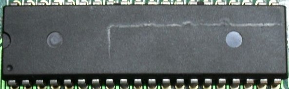 | |
| 23C269 | VRC2 | 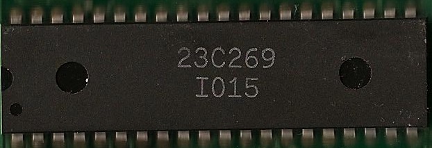 | µWire EEPROM interface works. |
| 23C3662 | VRC2 | 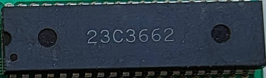 | Though known to be a VRC2 clone, the mirroring register only exists at $9000 like VRC4. µWire EEPROM interface works. |
| AX-40G | VRC2 | 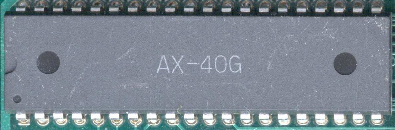 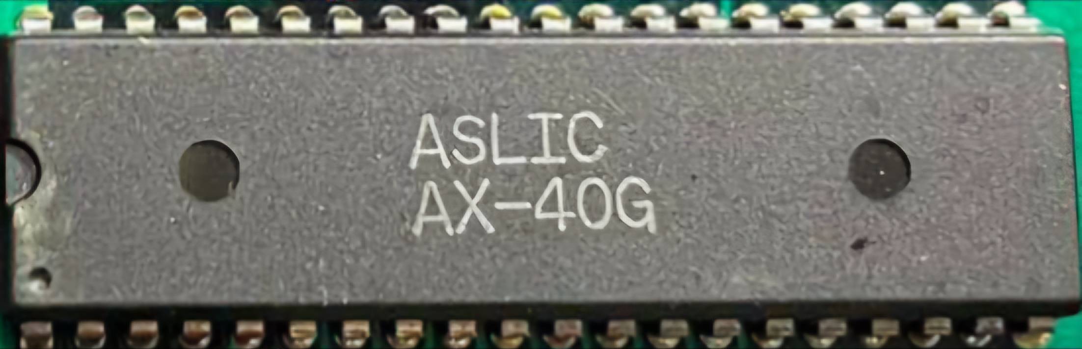 | |
| AX5705 | VRC2 | 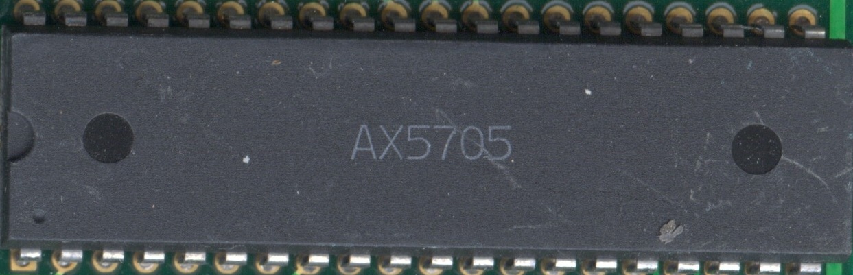 | µWire EEPROM interface works. Relabeled version of 23C269? |
| (nameless) | VRC4 |  | $F003 (IRQ Acknowledge) does not move the 'A' control bit to the 'E' control bit. |
| 23C3664 | VRC4 |  | |
| AX5208C | VRC4 | 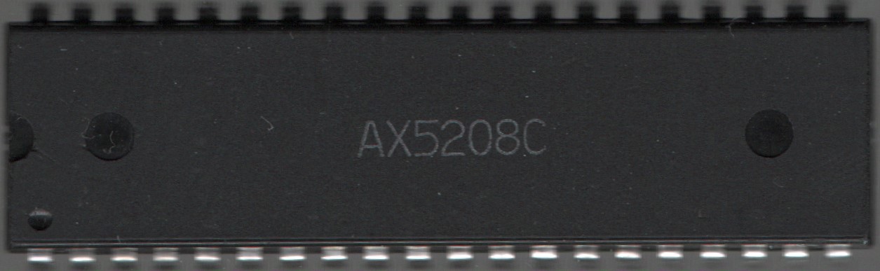 | WRAM is mapped at full $6000-$7FFF range, unlike the genuine VRC4 IC which only maps WRAM at $6000-$6FFF. /WR9003 pin is functional. |
| AX5208P | VRC4 | 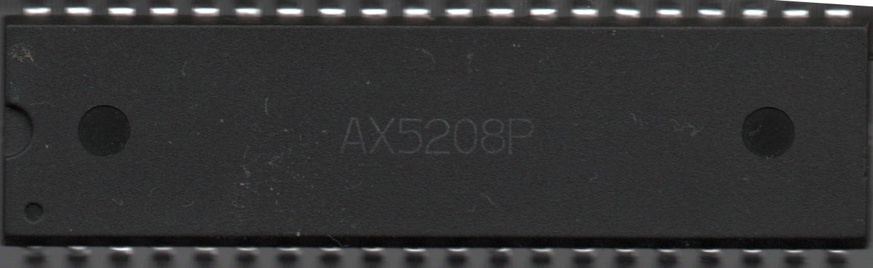 | Known to work differently compared to AX5208"C". Probably regarding to WRAM. WRAM responds at full $6000-$7FFF. /WR9003 pin is functional. |
| PT8155 | VRC4 | 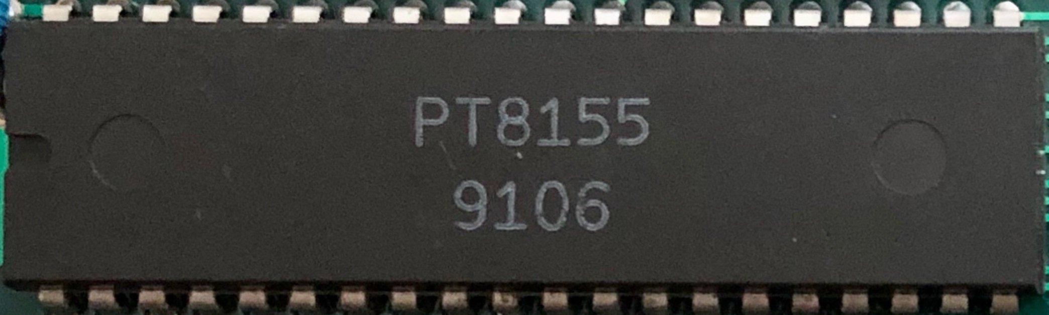 | This specific clone IC seems to have PRG A17 and/or CHR A17 (and maybe CHR A18?) pins either broken, repurposed or not connected at all, because at least one PCB with that chip (P-4073 PP-43KII, game Wai Wai World 2) contains additional logic to provide missing PRG A17 and CHR A17 lines. |
| V4 | VRC4 | 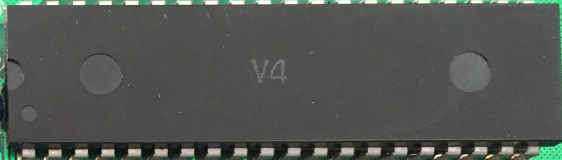 |