
CE Decoder
A 74LS139 decoder circuit generates the chip enables for the internal work RAM at $0000-$1FFF, the PPU at $2000-$3FFF, and PRG ROM at $8000-$FFFF.
The ‘139 (U3 in the schematic) has two halves, each of which has an enable input, two address inputs, and four enable outputs. The two halves work on the most significant bits (A15, A14, and A13) of the 2A03’s address bus.
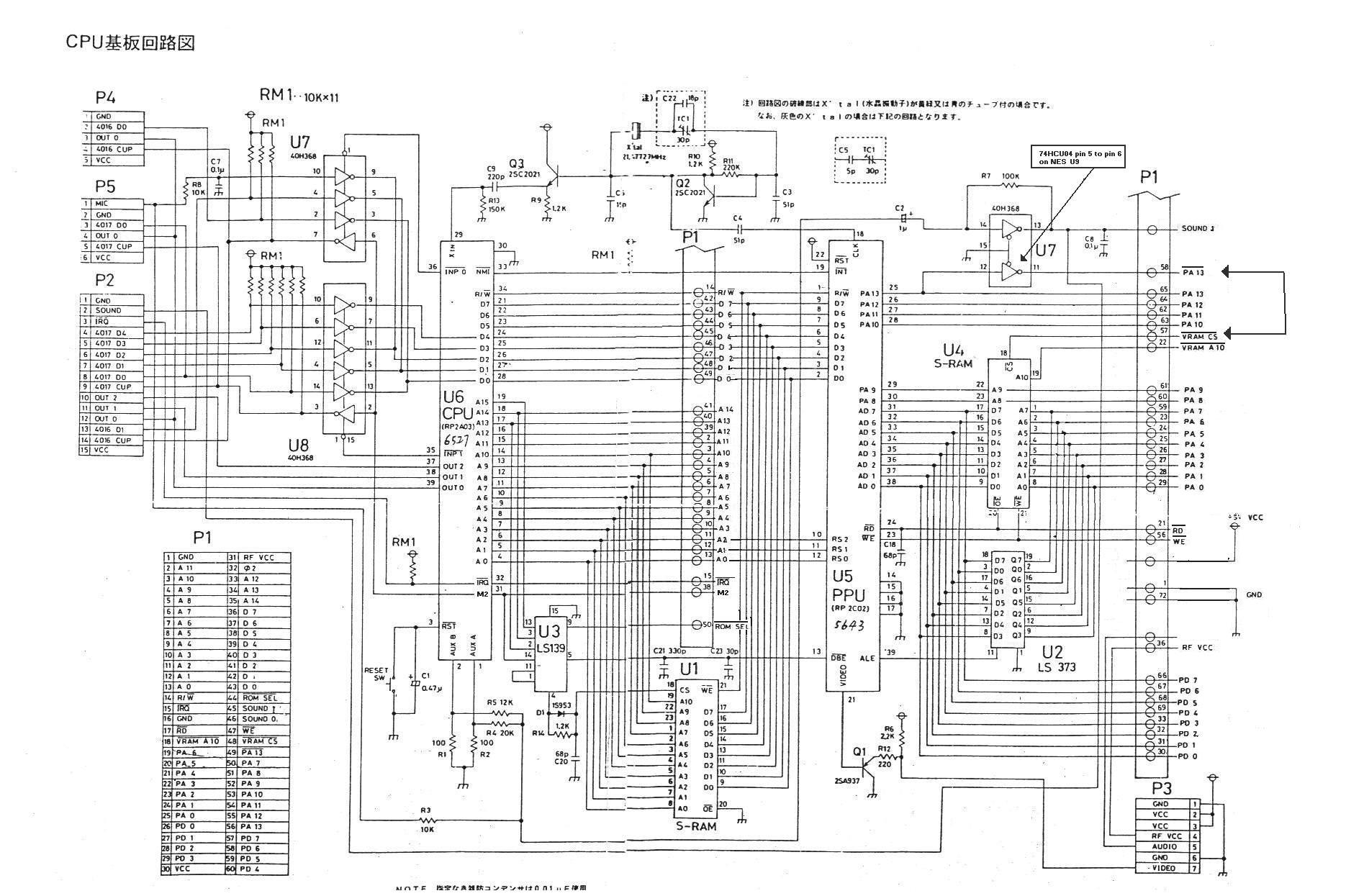
- One half combines M2 (the CPU clock) with A15 to produce /ROMSEL (M2 NAND A15) at $8000-$FFFF, a signal that enables PRG ROM on the vast majority of cartridges, and a signal that $0000-$7FFF is being accessed. You might call this /M07 = A15 OR NOT M2.
- The other half is enabled by /M07 and uses A14 and A13 to sort $0000-$7FFF into four smaller ranges. It produces four chip enable signals: $0000-$1FFF for work RAM, $2000-$3FFF for the PPU, and two that are not connected to anything ($4000-$5FFF and $6000-$7FFF).
These enable signals are active low, meaning they are driven to ground when the address is within the range and high when the address its outside the range.
The decoding is incomplete, producing address mirroring effects.
- Work RAM is 2 KiB, canonically at $0000-$07FF, and appears four times throughout $0000-$1FFF because A12 and A11 are connected to nothing while is selected.
- PPU registers are 8 bytes, canonically at $2000-$2007, and appear 2,048 times throughout $2000-$3FFF because A12 through A2 are connected to nothing while is selected.
The outputs that are low for $4000 and $6000 are not connected to SRAM (PRG RAM), which is decoded by the cartridge, nor APU registers, which are decoded internally by the 2A03.